Although there are simple DAC chips available for less than $2 USD, these may be hard to get at reasonable lead times, and at reasonable retail price. If the precision requirements are not very high, you may want to consider rolling your own using R/2R resistor network and 8-bit latch. This page describes such solution, and also gives some performance analysis results.
What is R2R network?
Well, it looks like this:
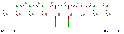
You connect your data bits from LSB to MSB, ground one end of the network, and get D/A conversion result as voltage from another end. Pretty simple. You can use discrete resistors, and there are SIL packages available containing the resistor network pictured above. They cost only cents if you find a reasonable supplier. I had one built from 10k and 20k resistors.
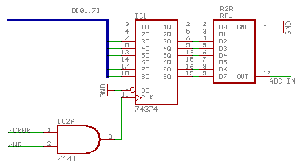
Schematics
I added a 74LS374 octal D-type flip-flop to my BASIC-52 core, and a 74LS32 to get the strobe. R2R network is directly wired to output pins, and output voltage was fed to ADC converter of my ADS1286 experiment.
The code
Using the D/A converter is ultimate in simplicity:
10 XBY(0C000H)=128
would set the output voltage to half of available range.
Performance
I then modified the ADC converter test code so that it creates a voltage ramp at DAC output and measures it using ADC, the output was logged to file and analyzed in Excel.
10 REM DAC test v1 15 GOSUB 1050 16 FOR J=0 TO 255 17 XBY(0C000H)=J 20 GOSUB 1200 30 PRINT J,AV 40 NEXT J 50 STOP 1000 REM start conversion 1010 PORT1=0FFH 1015 PORT1=07DH 1020 RETURN 1050 REM stop ADC 1060 PORT1=0FFH 1070 RETURN 1100 REM one clock, leaves clock high 1110 PORT1=07DH 1120 PORT1=07FH 1130 RETURN 1200 REM take ADC reading 1210 GOSUB 1000 1215 AV=0 1220 GOSUB 1100 : GOSUB 1100 : GOSUB 1100 1230 FOR I=1 TO 12 1240 GOSUB 1100 1250 BT=PORT1.AND.1 1260 AV=AV+AV+BT 1270 NEXT I 1280 GOSUB 1050 1290 RETURN
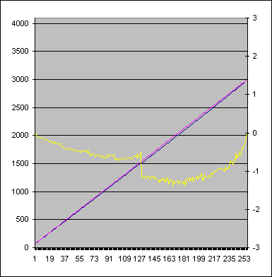
I ran the above program on two different 74LS374 chips, the graphs below show the result. Purple line shows the linear ramp the should have been output by DAC (ignoring the fact that LS technology chip does not run from rail to rail). Blue line shows the actual measured ramp. Yellow line shows error as percentage of available full scale. As you can see, the error is quite large.
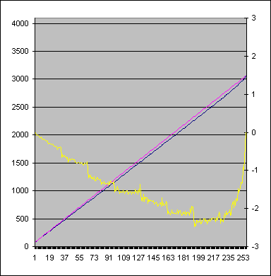
Second chip was much better, the only bit significantly off was MSB, hence the step in a middle of graph. Still, the error was about 1.4% which is adequate for lots of projects.
In general, TTL chips are not best for this kind of application. First, you cannot get them to give to full scale output to VCC. The outputs have resistors on high side, which combine with output transistor to make each output a little bit different than others. 74HCT374 which has CMOS outputs swinging rail to rail with only about 50 ohm Ron resistance is much, much better:
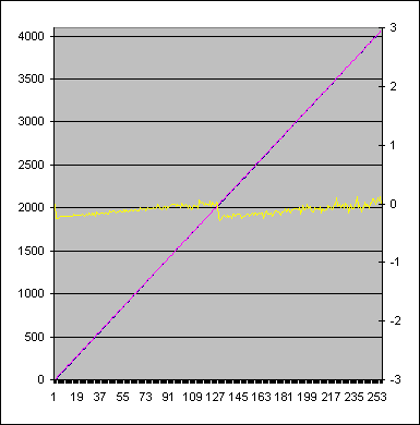
As you can see, HCT logic does indeed swing almost all the way from rail to rail (the actual ADC conversion results were from 0 to 4068) and error is less than 0.3%. This is pretty good. Notice the large amount of noise, especially on the higher output where the MSB outputs are less attenuated by resistor network. This can be cut down by proper analog power supply for flip-flops and ADC, or at least good power filtering. I did not bother.