After building my first 8052-BASIC project I learned that there is more to that Basic that shows up on a surface. The most important fact is that it looks for extension ROMin code memory space and if couple of bytes check out during boot, tries to call initialization code and does other interesting things in that ROM space. So the method to map 32K of RAM to both code and data space is not a very good idea at all, possibly resulting a crash at startup..
Below is a better memory map that the core implements:
| Addr | Data space (XBY) | Code space (CBY) |
| 0000 | RAM | on chip ROM |
| 2000 | RAM | Extension ROM |
| 4000 | RAM | Extension ROM |
| 6000 | RAM | RAM shared with data space |
| 8000 | PROG ROM | PROG ROM |
| a000 | PROG ROM | PROG ROM |
| c000 | I/O expansion | I/O expansion |
| e000 | I/O expansion | I/O expansion |
The address space is divided into 8 segments, last two are available for adding more memory or I/O devices. Address space is combined from 8000 as before, but the lower half is separated. As before, we have 32K of ram in data memory space. ROM space however is separate up to 6000, and includes 8K of on-chip ROM, 16K of extension ROM space, and from 6000 to 7FFF acesses data space RAM (so that we have a place where we can run native code from RAM, too). Extension ROM is where interpreter looks for it's extensions, custom input/output handlers and so on. You can, of course, store generally useful functions for your app in this ROM, too. PROG ROM is where 'PROG' and 'FPROG' instructions store Basic programs and interpreter settings, this ROM has a programming voltage supply to allow progrmming on board (as opposed to extension ROM which does not).
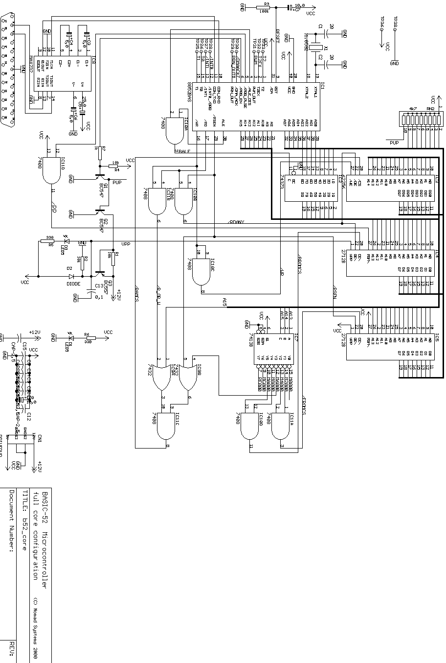
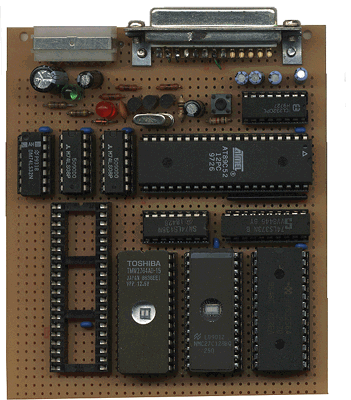
The schematics shows a Basic-52 micro with full memory configuration. For clarity, there is no expansion connector except that the unused control pins are attached to jumper pad.
IC7 divides the address space into 8KB chunks, which are then combined by IC11A to form expansion ROM chip select, and IC10D to form PROG ROM chips select. RAM chip select is a bit trickier, mainly because of the shared region at 6000H. IC7 output is first combined with code space read (indicating ROM space access). A15 signal is then combined with /R_OR_W signal indicating RAM access. Both are then combined, resulting in active low signal if either is true.
Programming voltage is switched using transistors, eliminating open-collector driver chip. As Q1 inverts the control signal, Q2 is needed to invert it again. Q3 then switches the programming voltage on and off, overriding +5V that is normally supplied to Vpp pin of EPROM via D2.
IC10C and IC11D are used as buffers, although buffering is probably unneeded, I had them left over so I wired them up this way.
Expanding the design
You can easily expand the circuit using Y6 and Y7 outputs of IC7 which decode addresses from C000H and E000H, either by using them directly as chip select signals or adding another 138 to further subdivide the block. /WR signal can be taken from IC10C output, as pure /RD is unbuffered, you may want to use IC10B output instead (this maps your device to both RAM and ROM space for reading, tho).
Couple of useful links
Interpreter source and binary code
HTML version of BASIC-52 reference manual
Copyright © Madis Kaal 2000-