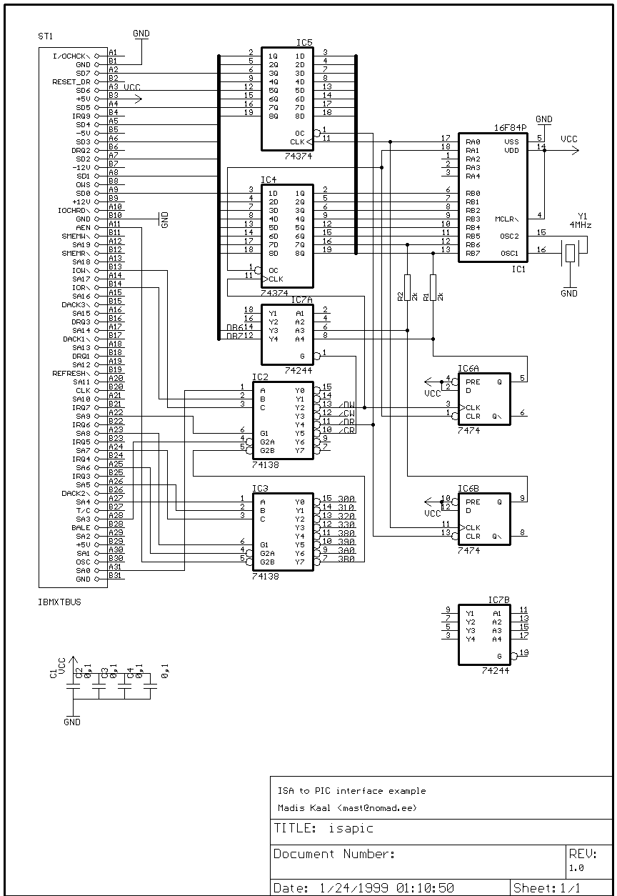
ISAPIC - ISA bus to microcontroller interfacing idea.This is an idea for interfacing PIC (or any other microcontroller) to ISA bus even if the MCU does not have special hardware. I have not yet tried out this exact circuit yet, but I have used couple of similar (a bit less elegant) designs successfully. This may be not be exactly what you are need, but at least it may give you some ideas. The circuit functions (or at least is supposed to function) as follows: IC2 and IC3 form an address decoder, by choosing an output pin of IC3, the device base address can be set to 300H,310H,320H,330H,380H,390H,3A0H, or 3B0H. IC2 looks at /RD, /WR and A0, and outputs four useful signals: /DW (data write), /CW (control write), /DR (data read), and /CR (control read). Data register is at base address, contol register is decoded at base+1. When the byte is written from ISA bus to base address, then /DW pulse captures the data to IC4, and also sets the output of IC6A, indicating data available. /CW signal is not used in this example. /DR signal enables output of IC5, which holds data which is written by PIC. /DR also clears the output of IC6B, indicating that PIC can output next byte. /CR signal enables IC7A that puts IC6 outputs to data bus. Bit7=1 indicates that the previously written data byte is not yet read by PIC, so it can be interpreted as BUSY bit. Bit6=1 indicates that PIC has written a value to data register that can be read - a DATA READY bit. DATA READY bit can be directly used as ISA IRQ output, if desired. Two more, application specific status bits can be easily added by using unused pins of IC7A, four more can be created by using IC7B. From PIC side, the interface uses PortB as data bus, but six unused pins can be used as inputs via resistors. Pulling RA1 low enables outputs of data register, allowing to read the data via PortB, and also clears the BUSY bit. There is a possibility of race condictions, because the BUSY bit is cleared when the RA1 goes low, the software on PC should include a sufficent delay to allow PIC to actually read the data and drive RA1 high again. To send data to ISA bus, PIC outputs it to PortB, then toggles RA0 low. Rising edge of the pulse will also set the DATA READY bit. Like with BUSY bit, a possible race exists, but this time the PIC side needs to be careful. However, the critical window here is ISA read cycle, so there is actually very small possibility that a 4MHz PIC can move fast enough to screw thigs up. Normally, unused pins of Portb (0..5) should be set to outputs all times, while RB6 and RB7, when set to inputs will allow reading of status bits (or even generate port change interrupt for PIC). It is unfortunate that this kind of interface eats up a lot of PIC pins, but most of PortB can still be used as input, and 3 PortA pins are available as outputs. If more outputs are needed, they can be easily created by adding one more 74374, and using one of PortA pins as strobe. This design can probably be easily converted into single programmable logic device, but I don't have any experience with them so I'll stick to this 6-chip interface for now. Copyright © Madis Kaal 2000- |