Hardware
You may want to check out the rfgenerator project for more modern version of the chip, and using it with AVR microcontroller
AD9835 is a DDS (direct digital synthesis) chip from Analog Devices. It contains a phase accumulator, sinewave table, and 10-bit D/A converter. In can be used for phase and frequency modulation by selecting the phase and frequency of the signal either under software control, or using I/O pins (4 phases, 2 frequencies). Although the chip is designed for RF applications, it makes a good audio frequency sinewave generator, too. The schematics below shows how to hook it up to 8052-BASIC chip.
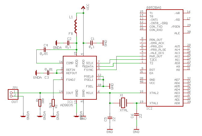
The circuit is quite straightforward. MCU clock is used as master clock for DDS, control interface is connected to PWM_OUT, T2EX, and T2. Phase and frequency selector pins are not used in this application, so they are tied to ground. Resistor and capacitor values are straight out of a datasheet schematics. Do filter the AVDD power supply, and keep the analog and digital grounds separated, connect them in single point as close to power supply as possible. The output voltage that is developed on R1 is between ground and REFIN (about 1.2V with internal reference used by connecting REFOUT to REFIN).
Construction tips
AD9835 comes in TTSOP-16 package (0.65mm pin spacing), and only that. You probably need some magnifying equipment to work with it (depending on your eyesight and steadiness of your hand). I just scanned the result with flatbed scanner at 1200dpi and examined the result. In general, the best option for prototyping in my opinion is a 'format conversion'.
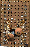 |
This is how I usually do it. I soldered the DIP-24 socket on veroboard, then cut a suitable size piece of a board and placed it over the socket. I then stuck a wire into socket through the board, soldered and trimmed the wire. The end result is a crude DIP-24 package. I then scraped the pads off from where the TTSOP case needed to go, and soldered wires to 'dip24' terminals from each of the pins. Finally I soldered power supply decoupling caps directly to the converter board. After you have soldered and visually examined the format converter, measure resistance from each pin against its neighbors to find any possible shorts. |
Beware of a probe poisoning!
AD9835 has a built-in 'suicide switch' which activates when you short the output to VDD or AVDD. All the magic smoke comes instantly out of a chip, and you have to start all over. Not to mention a loss of your hard-to-get chip.
The software
10 REM AD9835 control v1 15 REM reset chip 16 PRINT "Initializing..." 20 CW=0F800H : GOSUB 1000 30 CW=0B000H : GOSUB 1000 32 CW=05000H : GOSUB 1000 33 CW=04000H : GOSUB 1000 35 REM clear phase reg 0 40 CW=01800H : GOSUB 1000 50 CW=00900H : GOSUB 1000 55 REM set default frequency to 1000 Hz 60 F=1000 : GOSUB 2000 : GOSUB 3000 95 REM enable chip 100 CW=0C000H : GOSUB 1000 190 REM main loop 200 PRINT "Output frequency set to ",INT(FW)*CX,"Hz" 210 INPUT "Enter desired frequency (Hz)? ",F 220 GOSUB 2000 : GOSUB 3000 230 GOTO 200 999 END 1000 REM send CW to AD9835 1010 PORT1=0BFH : PORT1=0BBH : FOR I=1 TO 16 1013 BT=0 : IF CW>32767 THEN BT=1 1016 CW=CW.AND.7FFFH : CW=CW+CW 1020 PORT1=0BAH.OR.BT : PORT1=0B8H.OR.BT : PORT1=0BAH.OR.BT 1040 NEXT I : PORT1=0BFH 1060 RETURN 2000 REM calculate DDS freq register values to FH,FL 2001 REM desired frequency is in F 2020 CX=XTAL/(2**32) 2030 FW=F/CX 2035 FW=FW+0.5 2040 FH=INT(FW/65536) 2050 FL=INT(FW-(FH*65536)) 2070 RETURN 3000 REM program FREQ0 using FH,FL 3010 CW=FL.AND.255 : CW=CW.OR.03000H : GOSUB 1000 3020 CW=INT(FL/256) : CW=CW.OR.02100H : GOSUB 1000 3030 CW=FH.AND.255 : CW=CW.OR.03200H : GOSUB 1000 3040 CW=INT(FH/256) : CW=CW.OR.02300H : GOSUB 1000 3050 RETURN
As you can see, the code is not a rocket science either. At line 1000 there is a subroutine to send a 16-bit command word to AD9835. At line 2000 is a subroutine that calculates a 32-bit frequency word for a frequency given in variable F. The frequency word is left in FW as 32-bit value, and also split to two 16-bit values FH and FL. Finally, subroutine at line 3000 programs FREQ0 register with frequency word taken from FH,FL. Lines 20 to 50 contain the initialization code, after that the output frequency is set to 1000 Hz, and chip is taken out of a reset which enables the output.
The output
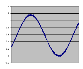
Below are the scope captures of output signal at 30kHz and 300khz. As you can see, 300kHz output only has about 11 discrete steps. Although the 30kHz signal shows no such steps, they are still there, but as there are 10 times more discrete steps, they are also 10 times smaller.
 |
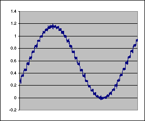 |
As the prototype was built on the same board with my other experiments, and power supply was not filtered except the decoupling capacitor, output is a bit noisy. Clearly, some sort of low-pass filtering is required to cut down the higher harmonics, and noise.
Filter
Filter is still cooking, will be presented when ready...